
Value Distribution of Advanced Packaging via AI Chip Teardown Analysis
If you want to understand where the real value sits in modern AI hardware, teardown analysis is one of the best tools available. Once you open up a flagship AI accelerator and examine its layers, you quickly discover that the package is no longer a supporting actor. It is a major source of cost, performance, and strategic value. In many cases, advanced packaging now accounts for a surprising share of total device value, rivaling or even surpassing the logic die in importance once HBM, interposers, substrates, and assembly are included.
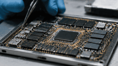
That is why AI chip teardowns are so revealing. They turn abstract industry debates into visible evidence. You can see the stacked memory, the interposer or bridge, the large compute die, the substrate, and the thermal structures that make the whole system work. More importantly, you can start to infer how much value each element contributes to the final product. Advanced packaging and heterogeneous integration are not just engineering choices anymore. They are value distribution engines.
Why Teardowns Matter
A teardown gives you a practical map of where engineering effort and money are concentrated. In a single AI chip package, the value is distributed across several layers:
- The leading-edge logic die.
- High-bandwidth memory stacks.
- The advanced packaging structure, such as a silicon interposer or fan-out platform.
- The substrate and redistribution layers.
- The thermal management system and mechanical support materials.
- The assembly, test, and yield loss absorbed during production.
When people talk about AI chips, they often focus on the compute die because that is the most visible piece of silicon. But teardown analysis shows that the package can carry an enormous amount of hidden value. In fact, for the highest-end accelerators, packaging and memory can dominate the economics of the final part. That makes advanced packaging a central, not peripheral, part of the chip’s value chain.
The New Cost Hierarchy
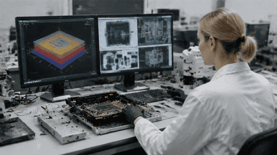
The old semiconductor cost hierarchy placed the logic die at the center and the package near the bottom. That hierarchy no longer fits leading AI hardware. Now the total cost stack often looks more like this:
- HBM or other advanced memory: very large share.
- Advanced packaging: a major share, especially in 2.5D and 3D designs.
- Logic die fabrication: still critical, but not always the dominant cost driver.
- Substrate, thermal materials, and test: smaller individually, but significant in aggregate.
This shift matters because it changes where value is captured. A chip maker no longer wins simply by designing the fastest core. It also has to secure memory supply, advanced packaging capacity, and reliable assembly. In many respects, the package has become a market gatekeeper. Teardown analysis makes that visible by breaking the chip into components and showing that the package is not an accessory but a core contributor to the final bill of materials.
What AI Chip Teardowns Typically Reveal
A typical AI chip teardown of a high-end accelerator shows a very dense system architecture. The main compute die sits at the center, often surrounded by multiple HBM stacks. These memory stacks are placed close enough to the logic die to enable enormous bandwidth. Underneath, there may be a silicon interposer, high-density organic substrate, or another advanced routing structure. Above or around that, the thermal solution must remove huge amounts of heat without interfering with electrical performance.
What becomes obvious very quickly is that the package itself is highly engineered. It is not merely a container. It is a precision-integrated platform. In some cases, the interposer and associated assembly flow are nearly as important to the end product as the compute die. The logic die can only perform as well as the package allows, and the package only works if all the surrounding materials, bonding techniques, and thermal paths are well controlled.
That is the real lesson of teardown analysis: advanced packaging has become a value amplifier. It increases the value of the compute silicon, but it also becomes a value center on its own.
Where the Money Goes
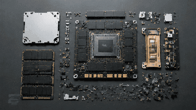
When analysts estimate AI chip costs, the discussion often focuses on wafer cost and memory cost. But teardown analysis reveals a more nuanced picture. Advanced packaging absorbs significant value in several ways:
- Interposer fabrication. Silicon interposers and high-density routing layers add cost and complexity.
- Assembly and alignment. Precise placement of multiple dies and memory stacks requires expensive equipment and process control.
- Yield loss. A defect in any key part of the package can lower the effective yield of the entire module.
- Thermal and mechanical structures. Lids, spreaders, adhesives, underfill, and related materials all contribute to final cost.
- Test and qualification. Multi-die packages require more sophisticated screening and validation flows.
That means the “package cost” in an AI chip is not a single number. It is a stack of multiple hidden costs that only becomes visible when you take the product apart. This is why advanced packaging can represent such a large share of total value. It is where complexity turns into money.
Heterogeneous Integration Changes the Math
Heterogeneous integration is one of the biggest reasons value distribution has shifted. Instead of building one giant monolithic die, companies now split functions across multiple dies built on different process nodes. That creates technical flexibility and can improve yield, but it also increases the packaging burden.
A heterogeneous package may include:
- A high-performance compute die on a cutting-edge node.
- HBM stacks manufactured and integrated separately.
- An I/O die on a more mature node.
- Signal routing and power delivery structures that tie them together.
From a value perspective, this means the package becomes the place where disparate pieces of silicon are transformed into a premium system. The more functions are split across dies, the more the package must do. That increases both engineering value and manufacturing value. Teardown analysis helps expose this by showing that the package is not just a technical necessity; it is a central part of the product’s economics.
2.5D vs. 3D in the Value Stack

The value distribution of advanced packaging depends heavily on the packaging style. In 2.5D systems, value is concentrated in the interposer, HBM integration, and high-precision assembly. In 3D systems, value shifts even more toward bonding technology, vertical integration, and thermal management. Each architecture distributes cost differently.
2.5D packaging often creates a large but still manageable cost addition because the dies remain side by side and the thermal challenge is less severe. 3D packaging can pack even more value into the stack because the technology is harder, more sensitive, and less mature. But it also introduces more yield risk and more expensive test requirements. That means 3D may carry a higher value concentration, but also a higher cost concentration.
Teardown analysis is useful because it lets you see not just what is inside the package, but what kind of technology stack is being paid for. A 2.5D package suggests one value distribution profile. A 3D stack suggests another. In both cases, the packaging technology itself is part of the premium product story.
Why Memory Matters So Much
One of the most striking things revealed by AI chip teardown analysis is the dominance of HBM in both cost and value. High-bandwidth memory is not just a supporting component. It is a core enabler of AI performance, and its proximity to the compute die is what makes the advanced package so valuable. Without HBM, the compute die cannot operate at the same bandwidth level.
That makes memory and packaging tightly linked. The package must place HBM stacks in the right geometry, with the right electrical characteristics, and with the right thermal path. This integration is expensive, but it is also what allows AI accelerators to reach their performance targets. In many leading devices, memory plus packaging can account for a very large share of total cost, which means the value of those layers is structurally high.
From a teardown standpoint, this is visible immediately. The memory stacks are prominent, the routing is dense, and the entire module is organized around getting data to and from memory as efficiently as possible. That is a strong clue that in AI chips, value follows bandwidth.
Packaging as a Strategic Moat
Another lesson from teardown analysis is that advanced packaging is not just about cost. It is also about strategic control. If only a few companies can manufacture high-end packages at scale, then the package becomes a bottleneck and a moat. That is exactly what has happened in AI hardware.
The ability to assemble a leading-edge accelerator depends on access to advanced packaging capacity, HBM supply, and the right substrates and materials. That means the organizations that control packaging can shape who ships, when, and at what volume. Teardown analysis makes that power visible because it shows how much of the final product’s value is locked up in the package.
In that sense, the value distribution is not just financial. It is strategic. Advanced packaging creates points of control in the supply chain, and those points are increasingly important in the AI era.
How Analysts Read the Package
When analysts perform teardown work, they are not just counting components. They are trying to infer the manufacturing decisions behind the product. The size of the interposer, the number of HBM stacks, the type of substrate, the bonding approach, and the thermal design all tell a story about value distribution.
A package with a large interposer and several HBM stacks suggests a high-value advanced packaging flow with significant performance-driven investment. A package with more compact integration and a less complex thermal stack suggests a different economic profile. Analysts use these clues to estimate where the money is going and where the supply chain is constrained.
That makes teardown analysis a bridge between engineering and economics. It turns physical evidence into a cost and value map.
Who Captures the Value?
One of the most interesting questions raised by AI chip teardown analysis is: who actually captures the value in the package? The answer is spread across several players. The chip designer captures value through system performance. The foundry or packaging house captures value through advanced assembly and integration. The memory supplier captures value through HBM. The substrate and materials suppliers capture value through enabling technologies. And the test and equipment ecosystem captures value through the manufacturing process.
In other words, advanced packaging redistributes value across the supply chain. It moves the economics away from a single die-centric model and toward a more distributed system. That is one reason the industry is so focused on advanced packaging now. It is not just about better performance. It is about where the value sits and who gets to hold it.
What This Means for the Future
As AI chips continue to grow in complexity, teardown analysis will become even more important. The next generation of packages will likely include more chiplets, more memory, more vertical integration, and possibly optical or other novel interconnect elements. That means the value distribution will become even more package-centric.
We are moving toward a world where the package may represent an even larger share of the final product’s value than many people expect today. That does not mean the compute die becomes unimportant. It means the compute die becomes one part of a larger, more integrated value system. Advanced packaging and heterogeneous integration are the structures that make that system work.
Teardown analysis will continue to serve as a reality check. It tells us where the complexity lives, where the cost accumulates, and where the strategic leverage sits. And increasingly, the answer is: inside the package.
Conclusion
Value distribution in AI chips has shifted dramatically because advanced packaging now carries so much of the system’s performance and cost burden. Teardown analysis makes that visible. It shows that the package is not just an enclosure but a major contributor to value creation, integration complexity, and supply chain strategy. HBM, interposers, substrates, thermal structures, and assembly all matter in a way they did not in older chip generations.
The big takeaway is simple. In modern AI hardware, the highest-value parts are no longer always the biggest dies. They are the layers and structures that turn separate dies into a functioning system. That is the true importance of advanced packaging and heterogeneous integration. The package is where the value is assembled, and teardown analysis is how we see it.





